Work Package 2: Light Readout
Objective: To develop advances in light readout for liquid detectors
Lead: Marcin Kuźniak (Astrocent, Nicolaus Copernicus Astronomical Center PAS)
Task 2.1: Increased sensor quantum efficiency
LXe and LAr emit in the challenging VUV wavelength range, where quantum efficiencies in PMTs are lower than for optical wavelengths. LXe experiments detect the emitted 178 nm light, where Hamamatsu photo-multiplier tube technology today achieves a maximum of ∼35% quantum efficiency (in the R12699-406-M4), with dark noise rate around 0.2 Hz/cm2, after-pulsing around 2% and transit time spread (single photon timing resolution) of 5.9 ns (FWHM). Silicon photo-multiplier (SiPM) approach these performances with the current state-of-the-art being the FBK VUV-HD3 and Hamamatsu VUV4 MPPC. The best quantum efficiency achieved in this technology at 178 nm is 20-25%, with the dark noise rate around 10-50 Hz/cm2 at LXe temperature dropping down by a factor of 10 at LAr temperature. For both solutions, the technology is front side illuminated Single Photon Avalanche Diode (FSI-SPAD) array with passive (resistive quenching). LAr emits around 128 nm and detectors typically employ large-area WLS thin films such that light can be detected at∼400 nm where the state-of-the-art in FSI-SPAD QE is ∼45% at LAr temperature. WLS films adds significant complexity for large-area readouts, and thus improving QE at 128 nm is strongly motivated. In general, SiPMs offer lower cost, higher fill factor, and better radiopurity – thus improving their performances is highly attractive, particularly for instrumenting large readout areas.
The frontier of this research now is developing solutions for overcoming the twin VUV issues of high reflectivity (>50%) and very shallow (nm scale) absorption depth in silicon. Such solutions have been demonstrated in charged coupled device (CCD) and other diodes but translating them to FSI-SPAD is difficult due to the pres- ence of non-silicon features needed for operating the SPADs, therefore motivating the development of back-side illuminated (BSI) SPADs. Our aim is to pursue the development of a new generation of SPAD arrays, reaching ∼50% efficiency with dark noise rate comparable to or lower than PMTs. In addition, new PMT solutions doing away with the dynode chain for amplification will also be investigated.
Optimised sensors and integration for maximum QE efficiency in the VUV wavelength range
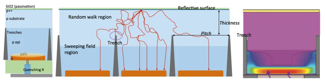
R&D focuses on optimising (i) SPAD and SiPM designs; (ii) anti-reflective coatings for the VUV and non-normal incidence; and, (iii) surface passivation for the VUV, including coatings and passivation. The strategies we propose to develop include drawing on the surface treatment and coatings technology developments for BSI-CCDs which achieve >40% quantum efficiency at 178 nm. The lack of structure on the exposed back side of the device maximises efficiency because the structure-less surface is easy to process for an optimally shallow junction and anti-reflective coating, and, there is no loss of efficiency due to front structure. For the objective of minimising dark count rate and correlated noise, we would operate at relatively low gain and fabricate this SPAD with trenches between pixels going all the way through the epi to minimise cross-talk. A conceptual scheme with 3 cells is shown in Fig. 2 (center). Simulation of this scheme, with n on p SPAD, shows optimal performance with pixel pitch as small as feasible (likely 5 µm), and super-thin p-substrate (ideally <= 1 µm). Institutes collaborating on this deliverable work with industry leaders FBK, Frauenhofer, Hamamatsu, and Teledyne-e2v, and would request funding for wafer production runs and coatings/passivation technology splits to support this development.
Integration also couples closely to the sensor development work. This R&D will develop strategies in collaboration with ongoing developments of custom SPAD/SiPM technologies at FBK, with the INFN-ARCADIA consortium, and with the Photon-to- Digital Converter (PDC) consortium who work with industry partner Teledyne-DALSA. 3D integration offers an attractive solution to achieve fast timing and manageable data rates. For large-area readouts, 2D integration of digital SiPMs is a cost-effective strategy that will be explored with VUV-optimised sensors. For rare event searches, BSI-SPAD integration has an added development challenge of achieving radiopure TSV bonding, but brings the potential advantage of up to 100% fill factor and an enhanced optical stack. Rapid feedback from qualification measurements early in the process is essential for integration R&D, for example qualifying SPAD arrays at the wafer level is necessary before packaging into detectors as the typical device yield ranges from 50% to 90%. The PDC instrumentation for wafer-level characterisation of SPAD reported in will be available to us in probing early prototypes of BSI-SPADs without requiring the complete processing (back-side thinning and processing) by illuminating the sensor from the front but producing electrons deep in the silicon as if they had been generated by photons impinging onto the backside.
Operational characterisation facilities for sensors in the VUV wavelength range
We plan to develop (i) detailed characterization setups for measuring photon detection efficiency; (ii) setups used to validate operation in liquid Argon and Xenon with particular attention to noise rates impacting SNR of single photon detection; and, (iii) underground setups used to validate operation in rare-event search experiments, both for liquid nobles (SoLAIRE) and water/liquid scintillator (BUTTON). We anticipate operating the characterisation facilities in a user-access model.
Task 2.2: Higher efficiency WLS/collection
Next generation LAr (and potentially some LXe) DM experiments, neutrino and neutrinoless double beta decay experiments will face the challenge of efficiently wavelength shifting and collecting scintillation light, emitted in the vacuum ultraviolet (VUV), from very large detector volumes. This will entail: enhancing properties of wavelength shifting (WLS) materials, needed in order to convert VUV to visible, where typically photosensors are more effiecient. While the WLS needs are highest for the 128 nm scintillation light of Ar, there could still be benefits to the overall light collection efficiency for the 175 nm scintillation light of Xe. R&D on production and installation of highly efficient WLS layers and/or reflective liners on inner surfaces of detectors with the surface area on the order of 10-1000 m2; and cost-effective light collector or concentrator systems coupled to photosensors (SiPMs or PMTs) and integrated with the overall detector design. In the new technique of opaque liquid scintillators the light is confined to a few cm volume near its creation point extracted by a lattice of WLS fibers running through the scintillator. In all cases extensive testing of such WLS materials, WLS or WLS-reflector surfaces and more complex light collector/concentrator systems in representative conditions is required. WLS also find application in liquid scintillators, water Cherenkov and WbLS detectors, enhancing the overall light yield by increasing the effective detection efficiency to the near UV light, constrained due to physical (UV absorption in optical windows) or budgetary (limited coverage with photosensors) reasons. In all types of detectors WLS with tailored slow time constants are also applicable for background mitigation via pulse shape discrimination.
In LAr-based DUNE and ARGO enhancing the light yield would lower the energy threshold extending the sensitivity to the few-MeV and few-keV region, respectively, and improving the detector performance for trig- gering, timing, calorimetry and background rejection. This R&D poses several challenges: the scintillation light from LAr is emitted in VUV where most materials are not transparent/reflective; the large volume of detectors requires cost-effective photon collectors; and for DUNE, specifically, the integration of photon detectors with the LArTPC field cage and charge readouts. DUNE’s photosensors are the so-called X-ARAPUCAs whose efficiency is 2-3% and R&D is required to optimize the X-ARAPUCAs design and increase its efficiency. In LXe, despite high reflectance of the PTFE sheets covering the internal walls, O(10%) of scintillation photons could be detected in XLZD, impacting the sensitivity to low-mass WIMPs Previous efforts on WLS coatings revealed issues with poor adherence and solubility.
Better scalable WLS and reflectors
R&D tasks include scaling up the TPB evaporation technology as well as more in depth studies of the reported issues with TPB stability in LXe and LAr, and ways to mitigate that issue (e.g. with protective coatings). Methods for embedding WLS in PTFE (or other polymers) include: PTFE/WLS mixture coating, mixing WLS with granular PTFE powder, and WLS diffusion into PTFE at elevated temper- ature. In parallel, intrinsically stable WLS polymeric films (e.g. polyethylene naphthalate, PEN), WLS-doped polymeric films and other novel candidate WLS (e.g. nanoparticles) will be further developed to better match the experimental requirements (higher efficiency, short re-emission time, radiopurity).
Optimized light collectors and concentrators
Light collectors and metalense-based light concentrators need identification and characterization of materials to increase photon collection. Particularly needed for the DUNE LArTPCs are: highly reflective/transmissive materials for the X-ARAPUCAs, highly reflective metals in the VUV for the detector components, and dichroic filters highly transparent to photons with wavelengths in the range between the VUV and a cut-off to wavelengths above it. In both contexts, cryogenic infrastructures for wavelength shifting efficiency and photon detection efficiency measurements and complete response characterization in representative conditions are needed, to provide data necessary for design optimization and simulations. In the case of the opaque liquid scintillator, we propose R&D on the fiber selection with high trapping efficiency and large attenuation length and optimization of the fiber coupling to the SiPM.